| ファイル | |
| 言語 |
英語
|
| 著者 | |
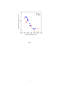
| 内容記述(抄録等) | As-grown and annealed samples of InAs layers grown by MBE at 150-350℃ were characterized by electron probe microanalysis (EPMA), high resolution X-ray diffraction (HRXRD), Hall measurements, and secondary ion mass spectrometry (SIMS). EPMA revealed that the As mole fractions in the layers grown at 150-200 ℃ are higher by about 0.5 % than those in the layers grown at 300-350 ℃. HRXRD measurements revealed that the layers grown at 150-200 ℃ have larger lattice spacings than the InAs substrate by about 0.02 %. Hall measurements revealed that the free-electron concentration in the layer grown at 200 ℃ is as high as 1.4×10^<19> cm^<-3> while such a high concentration of impurities cannot be detected by SIMS. Upon annealing at higher temperatures than 250 ℃, both the lattice spacing and the free-electron concentration of the layer grown at 200 ℃ were observed to decrease. These phenomena can be reasonably attributed to antisite As.
|
| 主題 | Semiconducting III-V materials
Molecular beam epitaxy
Point defects
|
| 掲載誌名 |
Journal of crystal growth
|
| 巻 | 301-302
|
| 開始ページ | 256
|
| 終了ページ | 259
|
| ISSN | 00220248
|
| 発行日 | 2006
|
| DOI | |
| DOI公開日 | 2013-04-01
|
| NCID | AA00696341
|
| 出版者 | Elsevier
|
| DCMI | text
|
| 資料タイプ |
学術雑誌論文
|
| ファイル形式 |
PDF
|
| 権利関係 | Copyright c 2006 Elsevier B.V. All rights reserved
|
| 著者版/出版社版 |
著者版
|
| 業績ID | e19781
|
| 部局 |
(旧組織)大学院総合理工学研究科
|