Properties of low-temperature grown InAs and their changes upon annealing
number of downloads : ?
Use this link to cite this item : https://ir.lib.shimane-u.ac.jp/24332
| ID | 24332 |
| File | |
| language |
eng
|
| Author | |
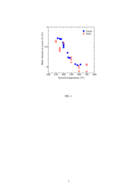
| Description | As-grown and annealed samples of InAs layers grown by MBE at 150-350℃ were characterized by electron probe microanalysis (EPMA), high resolution X-ray diffraction (HRXRD), Hall measurements, and secondary ion mass spectrometry (SIMS). EPMA revealed that the As mole fractions in the layers grown at 150-200 ℃ are higher by about 0.5 % than those in the layers grown at 300-350 ℃. HRXRD measurements revealed that the layers grown at 150-200 ℃ have larger lattice spacings than the InAs substrate by about 0.02 %. Hall measurements revealed that the free-electron concentration in the layer grown at 200 ℃ is as high as 1.4×10^<19> cm^<-3> while such a high concentration of impurities cannot be detected by SIMS. Upon annealing at higher temperatures than 250 ℃, both the lattice spacing and the free-electron concentration of the layer grown at 200 ℃ were observed to decrease. These phenomena can be reasonably attributed to antisite As.
|
| Subject | Semiconducting III-V materials
Molecular beam epitaxy
Point defects
|
| Journal Title |
Journal of crystal growth
|
| Volume | 301-302
|
| Start Page | 256
|
| End Page | 259
|
| ISSN | 00220248
|
| Published Date | 2006
|
| DOI | |
| DOI Date | 2013-04-01
|
| NCID | AA00696341
|
| Publisher | Elsevier
|
| DCMI | text
|
| NII Type |
Journal Article
|
| Format |
PDF
|
| Rights | Copyright c 2006 Elsevier B.V. All rights reserved
|
| Text Version |
著者版
|
| Gyoseki ID | e19781
|
| OAI-PMH Set |
Interdisciplinary Graduate School of Science and Engineering
|

